Facts · Systems · 7 cards

Hardware & GPUs

Chips the size of a stamp that cost as much as a car

Data wires per memory unit

One DDR5 memory stick64
One HBM3 stack1,024
HBM is fast because it is wide: one HBM3 stack has 1,024 data wires where a DDR5 stick has 64. Source: JEDEC JESD238 HBM3 standard

These facts come up in the course What AI Costs, where each one is explained step by step.

1

814 mm²

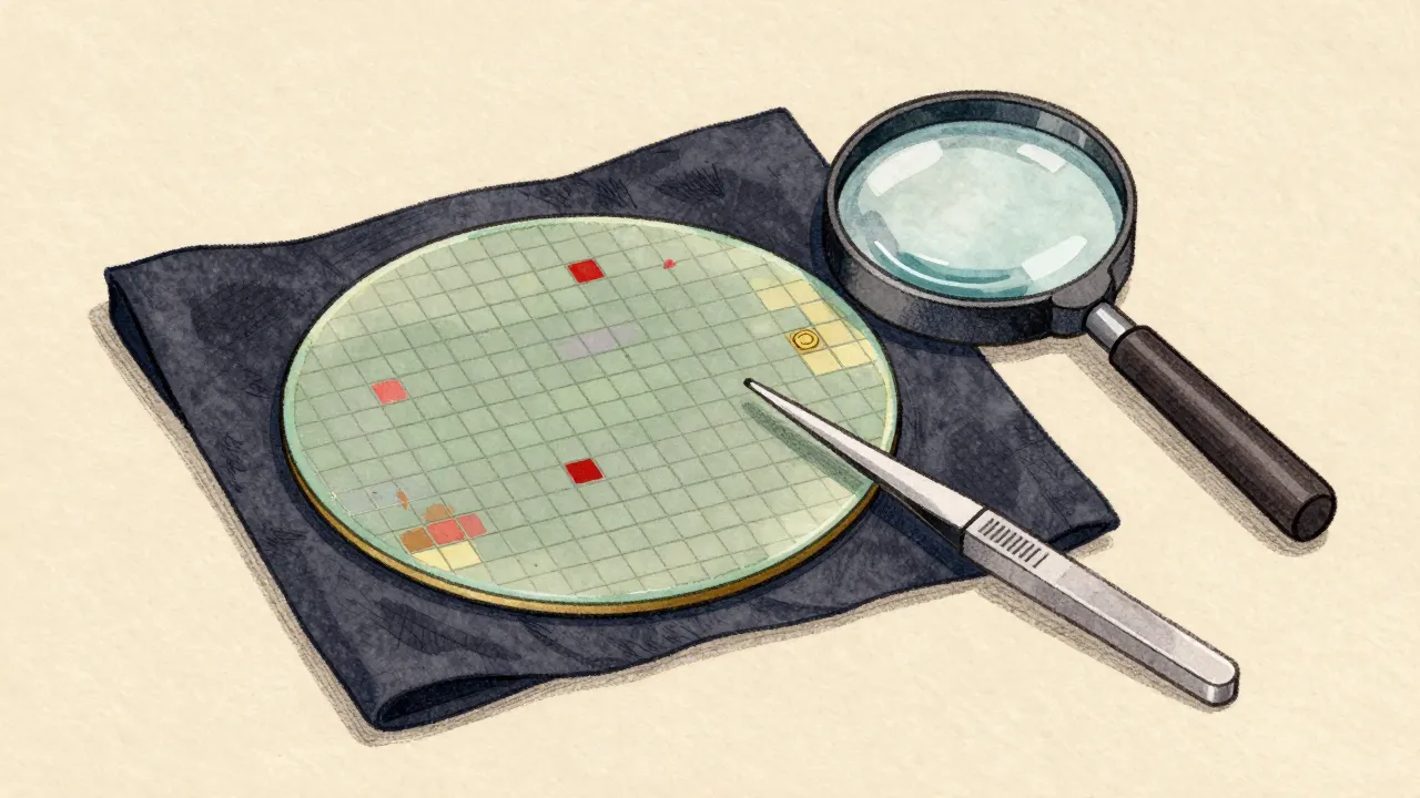
An H100 chip is barely bigger than a postage stamp

About 28.5 mm on a side, it carries 80 billion transistors. That is close to the largest rectangle a chipmaking machine can print in one shot.

How we got this number

The printing field of a lithography scanner is about 26 × 33 mm, or roughly 858 mm². At 814 mm², the H100 die uses almost all of it.

Source: NVIDIA, Hopper architecture in depth, 2022

2

208 B

Transistors in one 2024 Blackwell B200 GPU package

Since a single die cannot grow past the printing limit, NVIDIA joined two ~800 mm² dies with a 10 TB/s link so they behave as one GPU.

How we got this number

The H100 had 80 billion transistors on one die. The B200 puts two reticle-limited (maximum-size) dies side by side: 208 billion in total, about 2.6 times as many.

Source: NVIDIA, Blackwell architecture, 2024

3

~720 µm

Twelve memory chips stacked, thinner than a credit card

Each memory die in an HBM3E stack (fast memory beside the GPU) is ground thinner than a hair, with gaps of 7 µm between dies. Samsung fits twelve into the same height as eight.

How we got this number

A credit card is about 760 µm thick. The industry standard kept HBM3E stacks within 720 µm; for HBM4, with 12- and 16-high stacks, it was raised to 775 µm.

Source: Samsung, HBM3E 12H announcement, 2024

4

Data wires per memory unit

One HBM3 stack1,024 data wires
One DDR5 memory stick64 data wires
One HBM3 stack: 1,024 data wires; One DDR5 memory stick: 64 data wires.

HBM wins by being short and wide: a thousand-wire bus a few millimeters long instead of a narrow bus spread along a motherboard. HBM4 doubles the count to 2,048.

Source: JEDEC JESD238 HBM3 standard

5

2 miles

Copper cable inside one GB200 NVL72 rack

Roughly 5,000 cables link 72 GPUs through 18 switch chips, carrying 130 TB/s. NVIDIA says using copper instead of optical links avoids about 20 kW of power per rack.

Source: NVIDIA GTC 2024 keynote

6

Wait, really?

The H100 is built on a "4 nm" process. So its smallest parts are 4 nanometers wide?

Show the answer

No. "4 nm" is a name, not a measurement.

Node names stopped matching any physical feature years ago. In TSMC's 5 nm family, which includes the H100's 4N process, transistor gates sit about 51 nm apart. The name now roughly tracks transistor density.

Source: IEEE International Roadmap for Devices and Systems

7

Guess first

An H100 is rated at 700 W. About how much can one draw at most once its server and the building are counted?

  1. About 700 W, the rating is the whole story
  2. About 7 kW
  3. About 1.5 kW
Show the answer

About 1.5 kW

An eight-GPU server can draw up to 10.2 kW, or 1,275 W per GPU; cooling and power distribution add 10 to 20 percent. So 100,000 GPUs at full load need about 150 MW.

Source: Epoch AI, How much energy does ChatGPT use?, 2025